tl;dr: Built a functional scanning tunneling microscope. Need more robustness against mechanical noise sources & less janky.
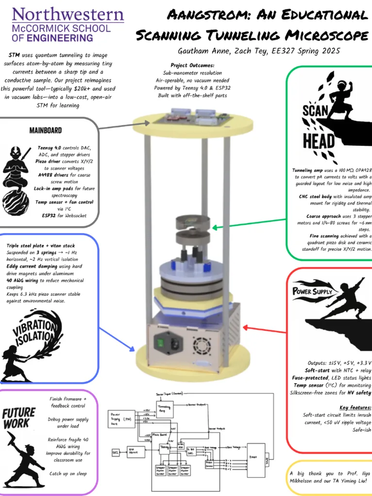
So, atoms exist. But, of course, seeing is believing (RIP Santa Claus), so I’ve decided to build an instrument that lets you image atoms. Specifically, this instrument is known as a Scanning Tunneling Microscope (STM). It belongs to a group of techniques known as scanning probe microscopy, where a small probe is scanned across a surface, obtaining information to post-process and render images. STM is a technique that takes advantage of quantum electron tunneling from an atomically sharp tip onto a conductive sample. Using some fancy feedback control of piezos, we can actually resolve individual atoms.
Typical commercial microscopes that are used in research labs cost upwards of $8,000 (for low end models), and ~$50,000 (for higher end models). If I were to drop a couple grand for funsies, I’d become even more of a burden on my parents. Thus, the project requirements are as follows:
- Low-Cost (~$300)
- Should be able resolve atomically flat conductive materials like HOPG, gold, silicon, specially prepared samples
- “Easy to use”
I came across Dan Berard’s (this guy is awesome) project my junior year of high school, but I lacked the prereq knowledge to build it then. This directory documents my journey attempting to make my own microscope (started 08/2024).
Some of the following pages sound super formal for blog posts, which is a result of me copying and pasting from my EE327 (Electronic System Design II) final report. Working on make it more concise…
Version 1 - Aangstrom (Updated 12/21/2025)
Overview
Design Overview + Constraints
Engineering Standards
Theory Of Operation
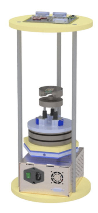
Mechanical Design Pages
Scan Head
Vibration Isolation
Electrical Design Pages
Power Supply
Tunneling Amplifier
Mainboard
Software Design Pages
Feedback Control
Firmware
Image Gallery - More coming soon!
HOPG (Highly Oriented Pyrolytic Graphite)
Example HOPG lattice (const. current mode, after some post processing to remove drift - attempting to streamline with Gwyddion).

Gold Films
Sputtered Platinum
Graphene on SiO2/Copper
Version 2
I’ve uncovered a couple of design headaches in V1: the “5V” stepper motors actually run much more smoothly at around 9 V, and those delicate 40 AWG wires—along with my patience—keep breaking far too easily.
Also, there’s an inherent coupling between ground and the scan head through the cable going to the outlet, so I’m thinking about transitioning to powering the system on a 20V Li-Ion drill battery (or LiFePO4 pack). I’m a little dissapointed the work spent on designing a custom power supply may be all for naught, but am glad I learned a ton.
I also started work on a more modular design for the scan head, enabling future integration of various types of microscopy, such an AFM head. See Dan Berard’s (the GOAT) project for more information.