Table of Contents
Open Table of Contents
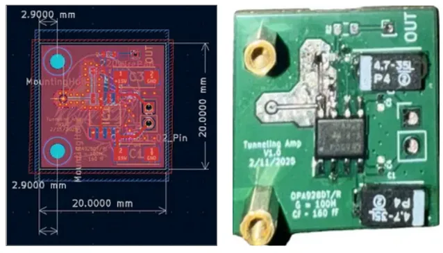
Description
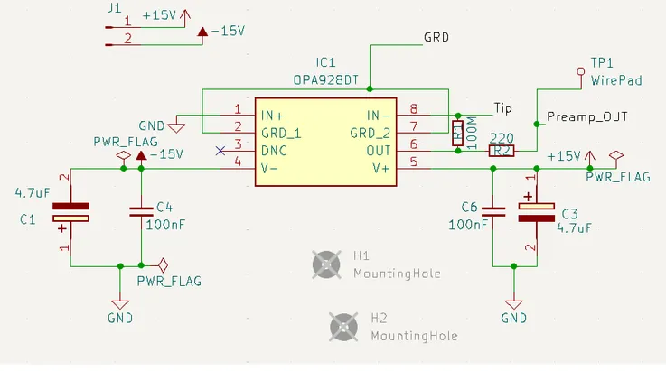
The tunneling current in a scanning tunneling microscope (STM) arises from the quantum mechanical tunneling of electrons between a conductive sample and a sharp metallic tip under an applied bias voltage. This current is typically in the picoampere (pA) to nanoampere (nA) range, often below the detection threshold of standard analog-to-digital converters (ADCs). Accurate measurement of this current necessitates a high-impedance, low-noise preamplifier with ultra-high gain and minimal input bias current. We therefore implemented a transimpedance amplifier (TIA) using the OPA928DT from Texas Instruments, optimized for ultra-low input bias current and low voltage noise density.
Amplifier Operation
The transimpedance amplifier converts an input current into a voltage via a feedback resistor , according to the ideal equation:
In our design, , resulting in a voltage gain sufficient to resolve currents as small as 10pA. The tip is connected to the inverting input of the op-amp, while the non-inverting input is held at analog ground (0V). The op-amp output feeds back through the large , and an additional small series resistor (220) at the output node helps isolate the amplifier from capacitive loading due to long cables, improving phase margin and overall stability.
Noise Considerations
The total noise in a transimpedance amplifier includes contributions from:
- The input current noise of the op-amp (),
- The input voltage noise () interacting with the source impedance,
- Thermal (Johnson) noise from the feedback resistor: where is Boltzmann’s constant, is temperature, and is the bandwidth.
Given the very large , thermal noise is significant and sets a practical limit on sensitivity. The OPA928, however, offers extremely low and , and its unity-gain bandwidth of 10~MHz ensures sufficient open-loop gain for our application.
Power Rails and Decoupling
Power to the amplifier is supplied through a two-pin header (J1) that delivers regulated V analog rails. Each rail is decoupled locally with a 4.7~F electrolytic capacitor in parallel with a 100~nF ceramic capacitor. This local bypass network helps reduce high-frequency power supply noise and prevents oscillations by stabilizing the op-amp power inputs.
Guarding and Layout Strats
Due to the extremely high input impedance and sub-nanoampere current levels, special layout techniques are essential to prevent signal corruption due to leakage currents. We employed a comprehensive guarding strategy:
- A driven guard pour surrounds all high-impedance input traces. This guard is actively driven to the same potential as the inverting input by the op-amp’s output, effectively eliminating potential differences that would drive leakage currents through PCB substrates.
- A continuous internal guard plane exists on an inner PCB layer directly beneath the signal trace. This shields against vertical leakage through the dielectric material.
- A via fence connects the guard pour across all PCB layers, forming a complete three-dimensional electromagnetic and leakage barrier.
- The solder mask was intentionally removed over the guard region to prevent capacitive charge accumulation on the surface, which could inject transient currents into the signal path.
- Ground pours are placed near—but electrically isolated from—the guard pour to minimize electromagnetic interference (EMI) and provide low-impedance return paths for surrounding circuitry.
Output and Interface
The amplifier’s output, labeled Preamp OUT, is routed to a test pad (TP1) and a shielded connector for delivery to the ADC on the STM mainboard. This output signal, a voltage proportional to tunneling current, is digitized and used in both imaging and feedback control. The output stage of the amplifier is configured to drive a capacitive load and is verified to remain stable under expected cable parasitics.