Table of Contents
Open Table of Contents
Description
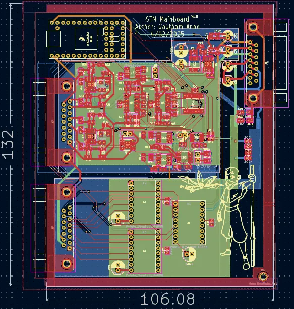
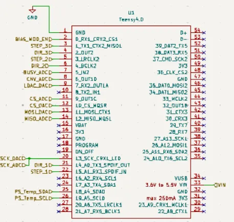
The STM mainboard serves as the central control and signal-processing hub for all active subsystems. It interfaces with the scanning, positioning, and signal acquisition circuitry and enables the feedback control that makes atomic-resolution imaging possible. The design is centered around a Teensy 4.0 microcontroller, selected for its low-latency digital control capabilities.
Digital-to-Analog and Analog-to-Digital Conversion
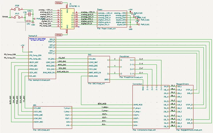
Precision in STM scanning requires fine control over the tip position and high-resolution measurement of tunneling current. To this end, the Teensy interfaces over a Serial Peripheral Interface (SPI) bus with:
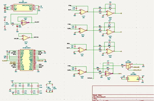
- A 4-channel Digital-to-Analog Converter (DAC), which generates analog control voltages , , and for piezoelectric actuation.
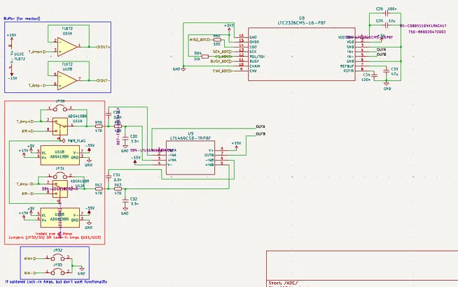
- A high-resolution Analog-to-Digital Converter (ADC), which samples the preamplified tunneling current signal .
The DAC outputs are updated in real time to synthesize raster scanning voltages or apply dynamic feedback corrections to maintain a constant tunneling current . Given the exponential dependence , even nanovolt-level changes in (which controls ) can modulate the tunneling current measurably. ADC (above) and DAC (below):
Sigma—Delta Modulation for DAC Output
Precise control of tip voltage is critical in STM operation due to the exponential dependence of tunneling current on tip–sample separation. While our mainboard uses a discrete DAC for analog control, the Teensy microcontroller also supports digital waveform synthesis via \emph{sigma—delta} () modulation, which we use for generating high-resolution bias voltages when hardware DAC channels are limited or when auxiliary analog outputs are needed.
Theory of Operation
modulation is a form of oversampled digital-to-analog conversion that achieves high effective resolution by shaping quantization noise out of the signal band. A basic first-order modulator consists of an integrator, a quantizer (e.g., 1-bit), and a feedback loop:
where is the input signal (scaled to [0,1]), is the 1-bit output, and is the internal integrator state. This results in an average output that closely tracks the input over time. When filtered with a low-pass analog filter (e.g., an RC or op-amp integrator), the pulse-density modulated (PDM) signal reconstructs the desired analog voltage:
for a sufficiently small and oversampling ratio.
Implementation on Teensy
On the Teensy 4.0, we implemented 1-bit modulation using a high-frequency PWM output (at 100–500~kHz) with a software-based accumulator:
This emulates the behavior of a 1st-order loop where {target_value} is a 16- or 24-bit fixed-point number and controls the resolution of the quantization threshold. The output is passed through a single-pole RC low-pass filter (e.g., , F) to yield an analog voltage:
Application of
- Generate programmable bias voltages across the sample,
- Output low-bandwidth feedback signals for coarse adjustment of tip height when dedicated DAC channels are unavailable,
- Provide test voltages or analog reference levels for board-level debugging.
Because the STM operates at relatively low bandwidth (scan frequencies Hz), the high oversampling rate and narrow analog bandwidth make modulation an ideal technique for generating low-noise, high-resolution voltages with minimal hardware overhead.
Advantages and Considerations
The approach provides:
- Higher effective resolution than PWM (12+ bits over time),
- Spectral noise shaping—quantization noise is pushed to high frequencies outside the STM bandwidth,
- Minimal digital logic requirements (integrator + threshold comparator).
However, careful analog filtering is essential to suppress out-of-band noise and ensure that high-frequency switching artifacts do not couple into sensitive analog circuitry (e.g., tunneling amplifier inputs). We currently are still in the process of implementing this step!
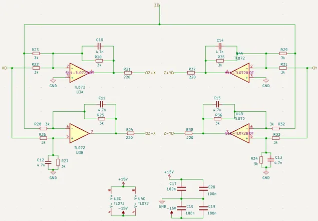
Piezo Driver and Unimorph Excitation
The DAC outputs , , and are routed to a custom piezo driver circuit that transforms these axis voltages into the composite combinations needed for the quadrant-driven unimorph disk piezo scanner. Specifically, we generate:
where to are the drive voltages applied to the four quadrants of the unimorph actuator. These combinations produce orthogonal in-plane and out-of-plane displacements, enabling full three-axis nanoscale control of the tip position.
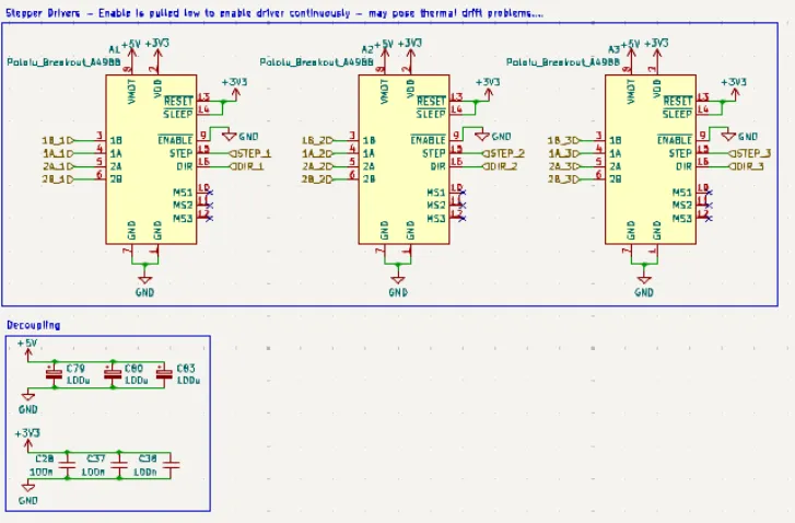
Coarse Positioning and Stepper Control
For coarse approach, the mainboard includes three A4988 stepper motor drivers, each controlling a 28BYJ-48 geared stepper motor driving a –80 fine-pitch screw. These motors are configured for microstepping, offering up to 2048 discrete steps per rotation. With a linear travel of 250~m/rev, the theoretical vertical step resolution is:
The Teensy generates direction and step pulses using its hardware timers, allowing precise synchronized control of all three coarse axes. By driving all three screws in phase, the entire scan head can be raised or lowered while maintaining parallelism with the sample surface.
Signal Integrity and Power Regulation
To preserve signal fidelity in a high-impedance, low-noise environment, the mainboard implements:
- Local decoupling at each IC with 100nF ceramics and 4.7F electrolytics,
- RC and ferrite bead filtering at sensitive analog interfaces,
- A high-accuracy REF102 voltage reference (10~V, ppm/C) for DAC reference input,
- Ground plane isolation between analog and digital domains, with a single-point star connection near the ADC/DAC.
Feedback Architecture and Thermal Monitoring
Real-time feedback control is implemented in firmware. The goal is to maintain the tunneling current at a setpoint by modulating . This is achieved using a proportional-integral (PI) controller:
This control signal is updated at fixed time intervals via Teensy hardware timers, ensuring deterministic timing critical for loop stability. The feedback bandwidth is designed to be below the mechanical resonance of the piezo stack to avoid excitation.
To support robust operation, the mainboard monitors its temperature using an LM75C digital sensor over an IC bus. The Teensy reads this temperature and adjusts the onboard cooling fan PWM accordingly. This thermal feedback loop can be described as:
where is a proportional gain and is the nominal threshold temperature.