Table of Contents
Open Table of Contents
Fabrication Steps
- Starts with blank wafer
- wafer is lightly doped into P-type substrate (can form NMOS transistor)
- Builds inverter from bottom up
- First step is formation of n-well
- Cover wafer with protective layer of glass
- Remove layer where n-well should be built
- Implant or diffuse n dopants (arsenic) into exposed wafer
- Remove SiO_2
Lithography exposes the photoresist through n-well mask, and strip off the photoresist using solvant. Then you etch the oxide with hydrofluoric acid (HF), which only attacks oxide where resist is exposed
n-well
- n-well is formed with diffusion or ion implantation
- Diffusion
- Places wafer in furnace with arsenic gas
- Heat until the arsenic gas diffuses into the Si
- Ion Implantation
- Blast wafer with beam of As ions
- Ions blocked by SiO_2, only enter the exposed silicon
Then you strip off the oxide usign HF, which is back to bare wafer with n-well.
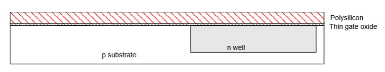
Polysilicon
- less than 20 Angstroms (6-7 atomic layers)
- CVD of Silicon Layer
- Place wafer in furnace with SiH_4
- forms many small crystals called polysilicon
- Heavily doped to be a good conductor
N-MOS - both source and drain are N, and P substrate in between.
Middle Work, Didn’t do yet…
Short Channel Effect
- IN small transistors, theres a depletion region in sources and drains (shortens the channel)
- This impacts the amount of charge required to invert the channel, and thus, makes V_t becomes a function of channel length
- In short channel effect: V_t decreases with smaller L, since leakage current increases, and transistor cannot be turned off…
Gates lose control of channel to due to source and drain, and V_t becomes smaller due to depletion