Table of Contents
Open Table of Contents
Introduction
VLSI (Very Large Scale Integration) techniques allow for the packing of billions of transistors together on chips. My CE391 (CMOS VLSI Circuits Design) class this past quarter was my first introduction to design techniques, complementary logic design, and transistor device physics. Throughout the course, I designed my own standard cells (Inverter, NAND2, NOR2, MUX2) from transistors to hierarchical blocks, which were reused other logic implementations (NAND2 usage in MUX2).
The culmination of the course was the design and layout of a complete 4×4 SRAM bank, built from the ground up using a standard 6T (six-transistor) SRAM bitcell in the FreePDK45 process. Rather than using pre-built memory macros, the project required a custom, hierarchical implementation starting from individual transistors and progressing up to a functional memory array.
6T-SRAM Bitcell
A 6T SRAM cell stores a single bit using a bistable latch, meaning it has two stable states and will remain in one of them indefinitely as long as power is supplied. The cell interacts with the outside world through two bitlines (BIT and BIT_B) and a wordline (WORD).
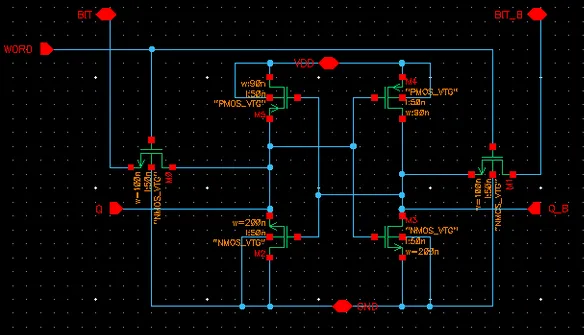 6T Transistor Cell Schematic
There are three modes of operations:
- HOLD (WORD = 0)
- When the wordline is low, the access NMOS transistors are OFF, which isolates the internal storage nodes from the bitlines. The two cross coupled inverters continuously reinforce each other, and the feedback loop ensures that the data is retained without any external inputs.
- WRITE (WORD = 1)
- To write data, the bitlines are actively driven:
- Writing ‘1’: BIT = 1, BIT_B = 0
- Writing ‘0’: BIT = 0, BIT_B = 1
Whem WORD is asserted, the access transistors connect the bitlines to the internal nodes. The stronger write drivers override the existing state, which makes the cross coupled inverters flip and settle into the new value.
- READ (WORD = 1, bitlines are precharged high)
Before a read, both bitlines are precharged to VDD. Then, WORD is asserted, and one of the internal nodes (storing ‘0’) slightly discharges its corresponding bitline, while the other bitline remains near VDD. This creates a small voltage differential between
BITandBIT_B, whcih is detected by the sense amplifer.
Transistor sizing needs to satisfy Pull-down NMOS > Access NMOS > Oull-up PMOS, which is required for both read stability (strong pull-down NMOS prevents cell from flipping during read) and write ability (access NMOS + bitline drivers must overpower weaker PMOS).
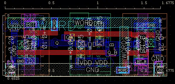 6T Cell Layout
Write Driver
The write driver is responsible for forcing a differential voltage onto the bitlines so that the SRAM cell can be overwritten. During a write, the input data (DATA) determines which bitline is pulled low. Thwe complementary bitline is held high and when W_EN is asserted, the driver becomes active.
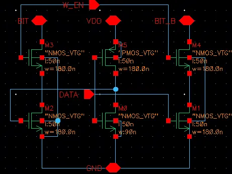 Write Driver Schematic
Once the wordline in the SRAM cell is asserted, the access transistors connect the bitlines ot internal nodes and the strong pull-down from the write driver overpowers the cell so that the cross-coupled inverters switch state.The key requirement is that write driver strength must be greater than the SRAM cell pull-up strength.
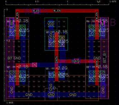 Write Driver Layout
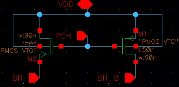
Precharge Circuit
The precharge circuit prepares the bitlines before every read by charging them both to VDD. This ensures a known starting condition so that even a small discharge can be detected by the sense amplifier.
 Precharge Schematic
When PCH is 0, the PMOS are turned ON, and both bitlines are pulled to VDD. When PCH is 1, the PMOS transistors turn OFF, which leaves the bitlines floating, and the SRAM cell can now discharge one of them during read.
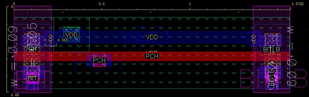 Precharge Layout
Clocked Sense-Amplifier
The sense amplifier detects and amplifes the small differential voltage during the read operations and converts it into a full-swing digital signal. Before sensing, both bitlines are precharged to VDD, and the read operation slightly discharges one of the bitlines (depending on the stored data), which creates a small . When SENSE_CLK is asserted, the sense amplifier is enabled, and it uses positive feedback (regeneration) to exponentially amplify the small voltage differentials between the two internal nodes until the circuit settles to one of two stable states.
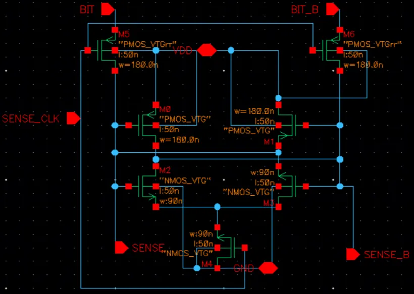 Sense Amp Schematic
Suppose intially the voltage at the left node, , is smaller than the voltage at the right node, . Then, drops slightly, which causes its PMOS to turn off more, and the opposite NMOS on the right side to turn on more. Because is slightly higher, this causes its PMOS to stay on more, and its NMOS to stay less ON. This creates a feedback loop where the lower node drops faster and the higher node rises/stays high.
Timing of SENSE_EN is important, as if it asserted too early, can be too small, and regeneration might pick the wrong side or become random. Thus, we need sufficient bitline discharge before the regeneration begins.
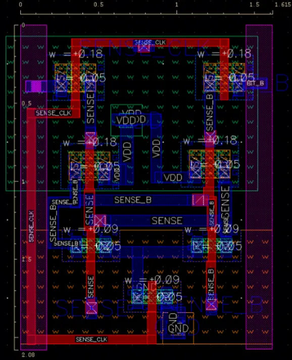 Sense Amp Layout
SRAM Bank and Testbench
The 4x4 bank stores 16 bits total. Each row shares a wordline, and each column shares a pair of bitlines (BIT/BIT_B).
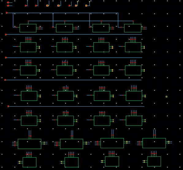
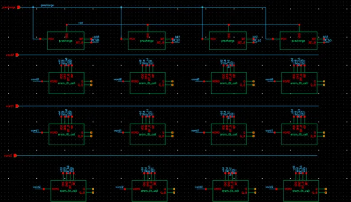 Bank Schematic
Operation is divided into three phases:
- Precharge
- All the bitlines are charged to VDD using precharge circuits
- Access
- A signel wordline (one row), is asserted, which connects 4 cells (one per column) to their respective bitlines
- Peripheral Actions
- Write: write drivers force values onto bitlines
- Read: sense amplifiers detect small bitline differences
In layout, I made sure to place sense amps at the bottom close to the state of the cells can be measured faster. Some performance limitations are that the bitline capacitance is large (since they are shared across 4 cells), discharge is small and slow, and the sense amplifier needs time to resolve. Thus, having a faster clock results in an insufficient , which results in a read failure.
The following testbench schematic is a top-level simulation setup used to verify the SRAM bank by generating the required control and data signals. Its jobs is not to store the data itslef, but to simulate the SRAM with timed input waveforms so the behavior of precharge, wordline activiation, and read and write operations can be observed in simulation.
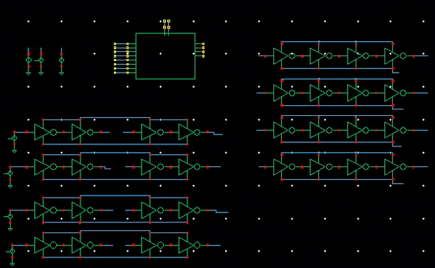
All the inputs pass through at least 1 inverter (Vpwl -> Inverter -> SRAM input), which models signal driving with (finite strength) and adds realistic delays. The SRAM block connects to bitlines, wordlines, control signals, and data inputs. Each output must be connected to 4 inverter loads (required by project specs). This models capacitive loads and prevents unrealistically fast transitions.
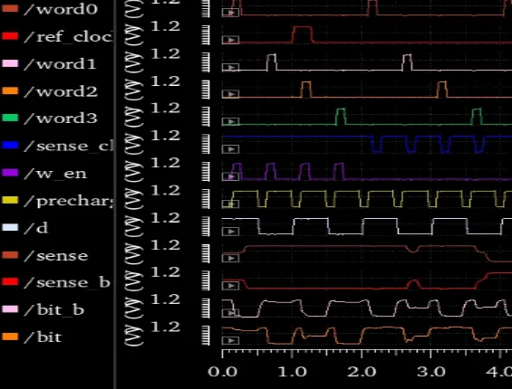
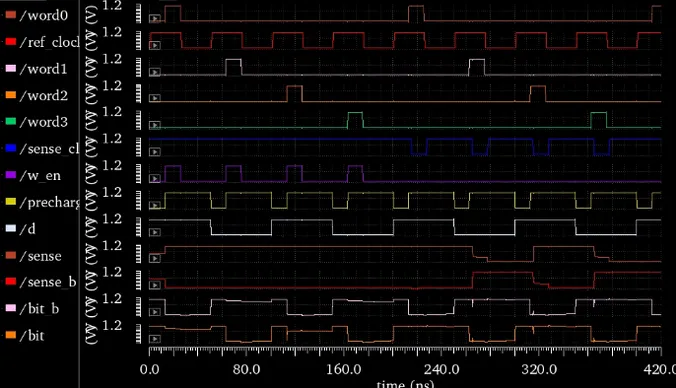 Before Layout Simulation - max clock speed was 1 ns before waveforms deteriorate significantly
After Layout Simulation - max clock speed was 2 ns before waveforms deteriorate significantly - read stability breaks