For my Mandelbrot Engine, I need to build a chain of modules to handle everything from pixel generation to high-speed electrical signaling. Because the Tang Nano 9k lacks a dedicated HDMI encoder chip, the FPGA has to do all the work. I’ll be describing the architectural design I implemented and debugged. The project’s repository is here.
Table of Contents
Open Table of Contents
HDMI Protocol
HDMI is a digital video + audio interface, so it should be relatively easy to drive from a modern FPGA (using a Gowin Tang Nano 9k). A standad HDMI connector has 19 pins. 8 of these pins form 4 TMDS differential pairs to transport the actual high speed video info:
- TMDS clock+ and clock-
- TMDS data0+ and data0-
- TMDS data1+ and data1-
- TMDS data2+ and data2-
The board I’m using already hsa the HDMI connector built in, so we can just configure 8 FPGA pins as 4 differential TMDS outputs. Because the Gowin GW1NR-9C lacks a dedicated HDMI PHY, we need to implement the TMDS serialization using OSER10 primitives and high-speed LVDS buffers.
Video Signal
I want to create a standard 640x480 RGB 24bpp @ 60 Hz video signals. This is 307200 pixels per frame, and since each pixel has 24 bits (8 per color chanel), at 60 Hz, the HDMI link transports 0.44 Gbps of data. However, video signals also have an “off-screen area” which is used by the HDMI receiver (monitor) for synchronization (described a bit more later), Thus, out frame is actually sent as an 800x525 frame.
For 60 fps, we require a 24.5MHz pixel clock, but since HDMI specifies a 25MHz minimum clock, we’ll get a 61 Hz output.
TMDS Signals
The FPGA has 4 TMDS differential pairs to drive. The TMDS clock is just the pixel clock, which runs at 25MHz. The other 3 pairs are the red, green, and blue 8bit signals, so we something like this…
However, things are a little more complicated, since HDMI requres a scrable of the data and add 2 bits per color lane, so we have 10 bits instead of 8, and the link ends up transporting 30 bits per pixel (24 + 2*3). The scrambling and extra bits are needed by the receiver to properly synchronize and acquire each lane.
video_timing.v
This module tells the monitor exactly where the electron beam (conceptually) is at any given nanosecond.
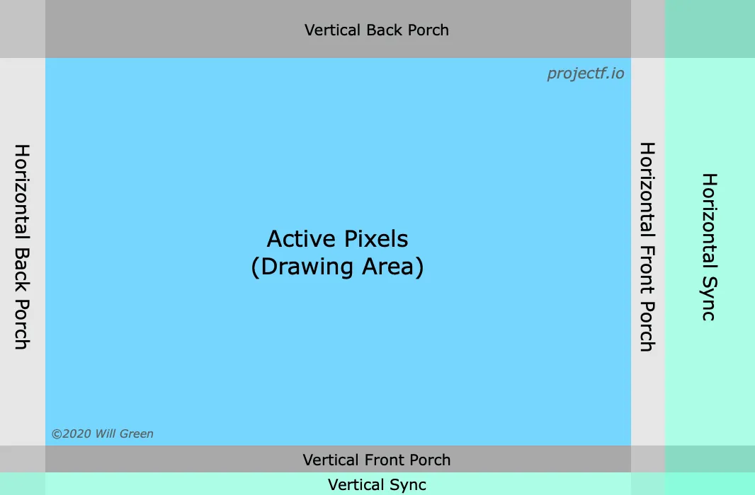
Anatomy of a Video Frame
Even though we only care about hte 640x480 pixels that show on screen, the timing geneator actually counts up to 800 horizontal pixels and 525 vertical lines. These extra areas are remnants of old CRT (Cathode Ray Tube) technology, where the electron beam needstime to reset from the right side of the screen back to the left. These portions are sectioned as follows:
How the Counters Work
This module uses two nested counters: h_cnt (horizontal) and v_cnt (vertical). The horizontal counter increments on every pulse of the 25.175 MHz pixel clock (counts from 0 to 799), and the vertical counter increments only when the horizontal counter finishes a full line (counts from 0 to 524).
if (h_cnt == H_TOTAL - 1) begin
    h_cnt <= 0;
    if (v_cnt == V_TOTAL - 1) v_cnt <= 0;
    else v_cnt <= v_cnt + 1;
end else h_cnt <= h_cnt + 1;
Signal Generation Logic
The module uses the current values of h_cnt and v_cnt to decide what the output signals should be:
active_video: This is a mask. It is High (1) only when both counters are within the visible 640x480 range. When low (0), the HDMI encoder will send “blank” black signals.h_syncandv_sync: These go Low (0) specifically when the counters are inside the “Sync Pulse” window as defined by the VGA standard.xandycoordinates: Provides the exact pixel address. For example, (x, y) = (320, 240) denotes the dead-center of the screen.
Full Implementation
module video_timing (
    input  wire pclk,
    input  wire rst_n,
    output reg  h_sync,
    output reg  v_sync,
    output reg  active_video,
    output reg  [9:0] x,
    output reg  [9:0] y
);
    // 640x480 @ 60Hz parameters
    parameter H_ACTIVE = 640;
    parameter H_FP     = 16;
    parameter H_SYNC   = 96;
    parameter H_BP     = 48;
    parameter H_TOTAL  = 800;

    parameter V_ACTIVE = 480;
    parameter V_FP     = 10;
    parameter V_SYNC   = 2;
    parameter V_BP     = 33;
    parameter V_TOTAL  = 525;

    reg [9:0] h_cnt, v_cnt;

    always @(posedge pclk or negedge rst_n) begin
        if (!rst_n) begin
            h_cnt <= 0;
            v_cnt <= 0;
        end else begin
            if (h_cnt == H_TOTAL - 1) begin
                h_cnt <= 0;
                if (v_cnt == V_TOTAL - 1) v_cnt <= 0;
                else v_cnt <= v_cnt + 1;
            end else h_cnt <= h_cnt + 1;
        end
    end

    always @(posedge pclk) begin
        h_sync <= ~(h_cnt >= (H_ACTIVE + H_FP) && h_cnt < (H_ACTIVE + H_FP + H_SYNC));
        v_sync <= ~(v_cnt >= (V_ACTIVE + V_FP) && v_cnt < (V_ACTIVE + V_FP + V_SYNC));
        active_video <= (h_cnt < H_ACTIVE) && (v_cnt < V_ACTIVE);
        x <= (h_cnt < H_ACTIVE) ? h_cnt : 0;
        y <= (v_cnt < V_ACTIVE) ? v_cnt : 0;
    end
endmodule
tmds_encoder.v
The goal of the tmds_encoder.v is to take the standard 8-bit color data and turn it into a 10-bit “wire-friendly” format. In DVI/HDMI, we don’t send raw bits because high-speed copper wire hates two things: too many transitions (which causes EMI/interference) and a DC imbalance (when there are more 1s than 0s, causing voltage to drift). My implementation solves this in 3 seperate stages.
1. Minimizing Transitions (8b to 9b step)
The first part of the code looks at the 8-bit color byte and decides whether to use XOR or XNOR logic to encode it:
- It counts the number of
1s in the data - If there are too many ones, or if the data starts with a
0, it uses XNOR logic to ‘flatten’ the data, making sure there are as few bit-flips (0-to-1 or 1-to-0) as possible - The 9th bit tells the monitor whether it used XOR (bit 9 is
1) or XNOR (bit 9 is0).
2. DC Balancing (9b to 10b step)
Even with minimum transitions, the data might stil send more 1s than 0s over time. This creates a “DC offset” on the wire. To fix this, the encoder keeps running a tally called bias (or commonly called disparity as). If the encoder has sent 100 more 1s than 0s, the bias is +100. If the next byte has more ones and the current bias is already positve, the encoder inverts the entire bias to send more zeroes instead. The tenth bit tells the monitor whether the byte is inverted to keep the wire happy (1), or whether it isn’t inverted (0).
3. “Control” Periods
HDMI isn’t just color. During the “Blanking” periods (when active_video is low), the monitor needs to see Sync pulses:
if (!active) begin
    case (ctrl)
        2'b00: tmds <= 10'b1101010100; // HSync/VSync encoding
        ...
When active is low, the encoder ignores color data and sends four specific 10-bit “Control Tokens.” These tokens are designed to be very easy for the receiver to indentify so it can stay “locked” to the pixel clock even when no image is being sent.
Full Implementation
module tmds_encoder (
    input  wire clk,
    input  wire [7:0] data,
    input  wire [1:0] ctrl,
    input  wire active,
    output reg  [9:0] tmds
);
    wire [3:0] n1d = data[0] + data[1] + data[2] + data[3] + data[4] + data[5] + data[6] + data[7];
    wire use_xnor = (n1d > 4) || (n1d == 4 && data[0] == 0);
    wire [8:0] q_m;

    assign q_m[0] = data[0];
    assign q_m[1] = use_xnor ? (q_m[0] ~^ data[1]) : (q_m[0] ^ data[1]);
    assign q_m[2] = use_xnor ? (q_m[1] ~^ data[2]) : (q_m[1] ^ data[2]);
    assign q_m[3] = use_xnor ? (q_m[2] ~^ data[3]) : (q_m[2] ^ data[3]);
    assign q_m[4] = use_xnor ? (q_m[3] ~^ data[4]) : (q_m[3] ^ data[4]);
    assign q_m[5] = use_xnor ? (q_m[4] ~^ data[5]) : (q_m[4] ^ data[5]);
    assign q_m[6] = use_xnor ? (q_m[5] ~^ data[6]) : (q_m[5] ^ data[6]);
    assign q_m[7] = use_xnor ? (q_m[6] ~^ data[7]) : (q_m[6] ^ data[7]);
    assign q_m[8] = use_xnor ? 0 : 1;

    reg signed [4:0] bias = 0;
    wire [3:0] n1q_m = q_m[0] + q_m[1] + q_m[2] + q_m[3] + q_m[4] + q_m[5] + q_m[6] + q_m[7];
    wire [3:0] n0q_m = 8 - n1q_m;

    always @(posedge clk) begin
        if (!active) begin
            bias <= 0;
            case (ctrl)
                2'b00:   tmds <= 10'b1101010100;
                2'b01:   tmds <= 10'b0010101011;
                2'b10:   tmds <= 10'b0101010110;
                default: tmds <= 10'b1010101011;
            endcase
        end else begin
            if (bias == 0 || n1q_m == n0q_m) begin
                tmds <= {~q_m[8], q_m[8], (q_m[8] ? q_m[7:0] : ~q_m[7:0])};
                if (q_m[8] == 0) bias <= bias + (n0q_m - n1q_m);
                else bias <= bias + (n1q_m - n0q_m);
            end else if ((bias > 0 && n1q_m > n0q_m) || (bias < 0 && n0q_m > n1q_m)) begin
                tmds <= {1'b1, q_m[8], ~q_m[7:0]};
                bias <= bias + q_m[8] - (n1q_m - n0q_m);
            end else begin
                tmds <= {1'b0, q_m[8], q_m[7:0]};
                bias <= bias - (~q_m[8]) + (n1q_m - n0q_m);
            end
        end
    end
endmodule
hdmi_top.v (NOT WORKING)
NOTE THAT THIS MODULE DOESN’T WORK. There’s some issues with this code that I had to spend some time debugging. Please reference my debugging section (later in this post) to get the working implementation.
The hdmi_top module is the Physical Layer (PHY) and the integration hub. It takes the internal logic (timing and colors) and prepares them for the physical HDMI cable. It’s primary job is to bridge the gap between the slow Pixel Clock (where logic operates) and ultra-fast Serial Bitstream (cable).
1. Clocking Architecture
HDMI requires two clocks working in harmony. In this design, I use Gowin rPLL to create:
- PCLK (25.175 MHz): The “Logic” clock. Every cycle, one pixel (RGB) is processed.
- FCLK (125.875 MHz): The “Serial” clock. This is exactly 5 times faster than PCLK.
Because we use DDR (Double Data Rate), we move two bits per FCLK cycle. Since 5 cycles x 2 bits/cycle = 10 bits, we send a ful 10-bit TMDS symbol for every 1 pixel clock cycle.
2. OSER10 Primitive
This primitve is a special hardware block inside the Gowin FPGA. I cannot write a standard always block to toggle pins at 250 MHz, since the fabric isn’t fast enough. Instead, we use OSER10 (Output Serializer).
- Input: It takes 10 bits all at once at the slow
PCLKrate - Output: It “shovels” them out of a single pin one by one at the high-speed FCLK rate.
- Clock lane: Note that we also serialize the clock itself. We send a 10-bit pattern of
1111100000, which creates a perfect square wave on the HDMI clock lane that the monitor uses to stay in sync.
3. Differential Signaling (LVDS)
HDMI doesn’t use standard 3.3V logic levels. It uses differential signaling, where two wires carry opposite signals (positive and negative). This helps cancel out electromagnetic noise. In the code, we use the TLVDS_OBUF primitve:
TLVDS_OBUF u_buf_data (.I(tmds_serialized), .O(tmds_d_p), .OB(tmds_d_n));This tells the Tang Nano hardware to take a single bit and drive it across two physical pins as a differential pair.
Full Implementation (NOT WORKING)
module hdmi_top (
    input  wire clk_27m,      // Crystal Oscillator
    input  wire rst_n,
    // HDMI physical pins
    output wire tmds_clk_p, tmds_clk_n,
    output wire [2:0] tmds_d_p, tmds_d_n
);
    wire pclk;   // 25.175 MHz
    wire fclk;   // 125.875 MHz (5x PCLK)
    wire pll_lock;

    // --- PLL Configuration ---
    // Use Gowin IP Designer to generate rPLL: 27MHz -> 125.875MHz (CLKOUT), 25.175MHz (CLKOUTD)
    GW_PLL u_pll (
        .clkout(fclk),     .clkoutd(pclk),
        .lock(pll_lock),   .clkin(clk_27m)
    );

    // --- Video Timing ---
    wire [9:0] x, y;
    wire h_sync, v_sync, active;
    video_timing u_timing (
        .pclk(pclk), .rst_n(pll_lock),
        .h_sync(h_sync), .v_sync(v_sync), .active_video(active),
        .x(x), .y(y)
    );

    // --- Placeholder Color Gen (Mandelbrot Hook here) ---
    // Integration Tip: Replace 'red', 'green', 'blue' with your Mandelbrot escape-time color map
    wire [7:0] red   = active ? x[7:0] : 8'd0;
    wire [7:0] green = active ? y[7:0] : 8'd0;
    wire [7:0] blue  = active ? x[8:1] : 8'd0;

    // --- TMDS Encoding ---
    wire [9:0] tmds_red, tmds_green, tmds_blue;
    tmds_encoder enc_r (.clk(pclk), .data(red),   .ctrl(2'b00),          .active(active), .tmds(tmds_red));
    tmds_encoder enc_g (.clk(pclk), .data(green), .ctrl(2'b00),          .active(active), .tmds(tmds_green));
    tmds_encoder enc_b (.clk(pclk), .data(blue),  .ctrl({v_sync,h_sync}), .active(active), .tmds(tmds_blue));

    // --- Serialization & Differential Buffers ---
    wire [2:0] tmds_serialized;
    wire tmds_clk_serialized;

    // Serialize Data Lanes 0, 1, 2
    genvar i;
    generate
        for (i = 0; i < 3; i = i + 1) begin : ser_data
            wire [9:0] tmds_val = (i==0) ? tmds_blue : (i==1) ? tmds_green : tmds_red;
            OSER10 u_oser (
                .Q(tmds_serialized[i]), .D0(tmds_val[0]), .D1(tmds_val[1]), .D2(tmds_val[2]),
                .D3(tmds_val[3]), .D4(tmds_val[4]), .D5(tmds_val[5]), .D6(tmds_val[6]),
                .D7(tmds_val[7]), .D8(tmds_val[8]), .D9(tmds_val[9]), .FCLK(fclk), .PCLK(pclk), .RESET(!pll_lock)
            );
            TLVDS_OBUF u_buf_data (.I(tmds_serialized[i]), .O(tmds_d_p[i]), .OB(tmds_d_n[i]));
        end
    endgenerate

    // Serialize Clock Lane (Sends a constant 1111100000 pattern at PCLK)
    OSER10 u_oser_clk (
        .Q(tmds_clk_serialized), .D0(1'b1), .D1(1'b1), .D2(1'b1), .D3(1'b1), .D4(1'b1),
        .D5(1'b0), .D6(1'b0), .D7(1'b0), .D8(1'b0), .D9(1'b0), .FCLK(fclk), .PCLK(pclk), .RESET(!pll_lock)
    );
    TLVDS_OBUF u_buf_clk (.I(tmds_clk_serialized), .O(tmds_clk_p), .OB(tmds_clk_n));

endmodule
IP Core Generator
Generating the rPLL
The code above requires the usage of a module called GW_PLL. This must be generated using the Gowin IP Core Generator because PLL settings are specific to silicon:
- Input Clock: 27 MHz
- CLKOUT (fclk): 125.875 MHz (drives the OSER10 serial side)
- CLKOUTD (pclk): 25.175 MHz (pixel clock, set the division factor 5 relative to CLKOUT)
- Duty Cycle: 50% for both
However, I ran into some issues (see below)!
Implementation & Debugging
Pain
Unfortunately, when I started setting up rPLL on Gowin’s IP Core Generator, I encountered a peculiar problem. Setting CLKOUT to be 125.875 MHz seemed to throw an error, like so:
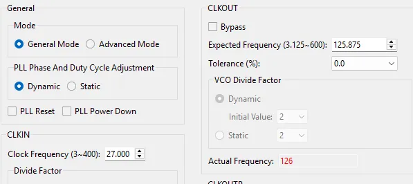
And while setting CLKOUT to 126 doesn’t throw an error, the derived CLKOUTD being 25.2 throws an error.
This is almost certainly due to how PLL hardware limitations. The Gowin PLL is an Integer-N PLL, not a true Fractional-N PLL that can hit arbitrary decimals. In addition, there are VCO (Voltage Controlled Oscillator) range constraints, and PFD (Phase Frequency Detector) Limits.
Thus, changing the fast clock (CLKOUT - serial) to 504 MHz and the pixel clock (CLKOUTD) to 25.2 MHz seemed to make the generator happy. However, now my serialization ratio is 20:1 instead of the original 5:1. Thus, I used the CLKDIV Primitive to ‘downsample’ nad
More Pain
After a decent bit of debugging, I realized I’m an idiot. My implementation of hdmi_top.v was failing due to clock phase misalignment (I skewed it up). I generated the Pixel Clock (25.2 MHz) and the Serial Clock (126 MHz) as two seperate outputs from the PLL:
- Path A: PLL - Internal Divider -> CLKOUTTD pin -> OSER10
- Path B: PLL -> VCO -> CLKOUT pin -> CLKDIV -> OSER10
So even though the logic was all sound, Path A and Path B have slightly differnt lengths and physical delays. This means the rising edge of Pixel Clock arrived slightly early or late relative to the Serial Clock. THE OSER10 tried to grab the data, but actually missed the window and sent garbage out.
The Gain
The way I fixed this issue was through “daisy-chaining” my clocks together:
- Path: PLL (504 MHz) -> CLKDIV (126 MHz) -> CLIKDIV (25.2 MHz)
By deriving the slow clock directly from the fast clock, I mechanically lock their phases together. The 25.2 MHz basically ‘ticks’ every 5 pulses of the 126 MHz clock. This guaruntees that the
OSER10grabs the data at the correct time.
In future projects, I do plan to try other fixes that are more ‘jank’ but functionally perform similar. For example, I could add a specific delay to either one of the clocks to introduce an offset to match phases. I also haven’t really used Gowin’s Timing Analyzer, which is something I want to learn to do.
Working hdmi_top.v!
module hdmi_top (
input wire clk_27m,
input wire rst_n,
output wire tmds_clk_p, tmds_clk_n,
output wire [2:0] tmds_d_p, tmds_d_n
);
wire vco_fclk; // 504 MHz
wire ser_fclk; // 126 MHz
wire pclk; // 25.2 MHz
wire pll_lock;
Gowin_rPLL your_pll_inst (
.clkin(clk_27m),
.clkout(vco_fclk), // 504 MHz
.lock(pll_lock),
.reset(!rst_n) // Check your IP: usually active high reset
);
//Serial clock
CLKDIV #(.DIV_MODE("4")) u_div_serial (
.CLKOUT(ser_fclk),
.HCLKIN(vco_fclk),
.RESETN(pll_lock)
);
// pixel clock
CLKDIV #(.DIV_MODE("5")) u_div_pixel (
.CLKOUT(pclk),
.HCLKIN(ser_fclk), // Chain from the serial clock
.RESETN(pll_lock)
);
// Video Timing
wire [9:0] x, y;
wire h_sync, v_sync, active;
video_timing u_timing (
.pclk(pclk),
.rst_n(pll_lock),
.h_sync(h_sync), .v_sync(v_sync), .active_video(active),
.x(x), .y(y)
);
// Fixed Color Test (Half Red and Half Blue)
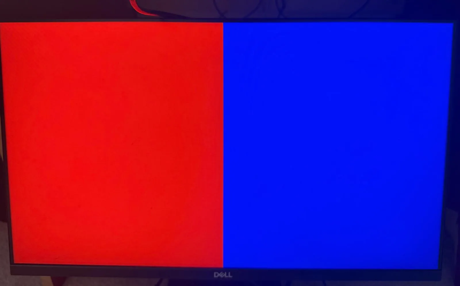
wire [7:0] red = active ? (x < 10'd320 ? 8'hFF : 8'h00) : 8'd0;
wire [7:0] green = 8'd0;
wire [7:0] blue = active ? (x >= 10'd320 ? 8'hFF : 8'h00) : 8'd0;
// TMDS Encoders
wire [9:0] tmds_red, tmds_green, tmds_blue;
tmds_encoder enc_r (.clk(pclk), .data(red), .ctrl(2'b00), .active(active), .tmds(tmds_red));
tmds_encoder enc_g (.clk(pclk), .data(green), .ctrl(2'b00), .active(active), .tmds(tmds_green));
tmds_encoder enc_b (.clk(pclk), .data(blue), .ctrl({v_sync,h_sync}), .active(active), .tmds(tmds_blue));
// Serialization
wire [2:0] tmds_serialized;
wire tmds_clk_serialized;
genvar i;
generate
for (i = 0; i < 3; i = i + 1) begin : ser_data
wire [9:0] tmds_val = (i==0) ? tmds_blue : (i==1) ? tmds_green : tmds_red;
OSER10 u_oser (
.Q(tmds_serialized[i]),
.D0(tmds_val[0]), .D1(tmds_val[1]), .D2(tmds_val[2]), .D3(tmds_val[3]), .D4(tmds_val[4]),
.D5(tmds_val[5]), .D6(tmds_val[6]), .D7(tmds_val[7]), .D8(tmds_val[8]), .D9(tmds_val[9]),
.FCLK(ser_fclk), // 126 MHz
.PCLK(pclk), // 25.2 MHz
.RESET(!pll_lock)
);
ELVDS_OBUF u_buf_data (.I(tmds_serialized[i]), .O(tmds_d_p[i]), .OB(tmds_d_n[i]));
end
endgenerate
// Clock Lane
OSER10 u_oser_clk (
.Q(tmds_clk_serialized),
.D0(1'b1), .D1(1'b1), .D2(1'b1), .D3(1'b1), .D4(1'b1),
.D5(1'b0), .D6(1'b0), .D7(1'b0), .D8(1'b0), .D9(1'b0),
.FCLK(ser_fclk),
.PCLK(pclk),
.RESET(!pll_lock)
);
ELVDS_OBUF u_buf_clk (.I(tmds_clk_serialized), .O(tmds_clk_p), .OB(tmds_clk_n));
endmoduleHere’s the logic output of synthesis:
Example Output
Yay! This worked out! Here is a test image of a half red / half blue screen. Stay tuned for my Mandelbrot Engine! I also have a fun project I’m working on (a DLP Maskless Lithography system) that will need to make use of this driver (although implemented on an FPGA with more LUTs).