Table of Contents
Open Table of Contents
Introduction
This is my final report, titled “Review of Quantum Defect Sensors for Magnetometry: A Case Study of Nitrogen-Vacancy Centers and 2D Hexagonal Boron Nitride”, for my EE381 (Electronic Properrties of Materials) course at Northwestern. My group members were Nolan Hannnan, Samuel Jung, and Bhavana Panchumarthi.
Abstract
Nanoscale magnetometry has an array of important applications in biomedical imaging, spintronics, and the continued study of physics and material science. While an array of magnetometry techniques have been used in these fields, including superconducting quantum interference devices (SQUIDs), optically pumped magnetometers (OPMs), microscopy based on magnetic force or Lorentz transmission electrons, and magnetoresistance, the emergence of two types of sensors using optically detected magnetic resonances (ODMR) offer potential for greater sensitivity, reduced cooling requirements, and even 3D vectorial detection [1], [2], [3], [4]. This paper will focus on the function and applications of negatively charged nitrogen-vacancy (NV–) diamond centers, and the emerging technology of hexagonal boron nitride (hBN), with some review of classical sensors.
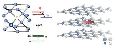 Figure 1: Left shows a nitrogen-vacancy center in diamond [5]. Right shows a spin defect located within hexagonal boron nitride [4].
Importance and Applications
The primary advantages of NV– magnetometers come in the form of their high sensitivity and ability to function under ambient conditions. Studies have found that for AC sensing, single NV– centers in highly pure diamond can achieve sensitivities of 30 nT Hz-½ with sensitivities down to 4.3 nT Hz-½ being possible when using isotopic engineering. Such sensitivities are possible at room temperature under ambient pressure [6]. Even for DC sensing, it has been demonstrated that sensitivities as low as 63 nT Hz-½ may be possible (when paired with giant magnetoimpedance effects) [7]. With such sensitivities, and the high spatial resolution of NV– centers (which has been shown to be as low as 8.9 nm with a strong magnetic field gradient), it may even be possible to measure the field of single electron spins. Lastly, sensitivities may be improved further, at the cost of spatial resolution through the use of NV– ensembles in a volume of diamond [6].
Research on hBN shows that it is currently less sensitive (with DC sensitivity as low as 1.5 uT Hz-½) [4]. This sensitivity may make hBN unsuitable for certain applications, such as magnetoneurography, which often requires sub-picoTesla sensitivities [1]. However, the advantages of hBN are found in its potential for vectorial sensing, increased stability under off-axis fields, and integration with 2D materials. Using two known magnetic “bias” fields, the three components of the target field can be determined exactly, without extrapolation, using a single hBN spin defect. Additionally, while NV– sensor readings degrade with an off-axis field of about 10 mT or higher, hBN sensors retain accurate function with transverse fields of over 150 mT. Thus, considering hBN sensors can also operate at ambient temperature and pressure, they are suitable for operation in a wider array of conditions than NV– center devices. Lastly, hBN is itself a 2D material, allowing for easy implementation with other 2D structures [4].
One application of NV– centers – in magnetoneurography – would allow for more accurate and less invasive measurement of nerve locations during surgeries. Use of NV– center magnetometry, as opposed to current electrical stimulation techniques, allows for a more generalizable approach, which is less susceptible to errors from tissue differences in different patients. Additionally, NV– centers greatly increase signal to noise ratio by being able to be positioned much closer to the source of the field, compared to other magnetometers [1]. Another application is the detection of magnetic domains and spin textures in the development of spintronic devices, enabled by the nanoscale spatial resolution of NV– sensors [2]. A final application of NV– centers is the further study of physics. Similar to their application in spintronics, the use of nanoscale spatial resolutions allows for the study of domain walls in ferromagnetic (FM) and antiferromagnetic (AFM) materials, and skyrmions. They may also be used for study of superconductors, with regard to both the Meissner effect and vortices in type-II superconductors [3]. While hBN does not have a significant number of applications currently, as there are a number of hurdles it must still overcome, there is an array of potential applications that may be possible with further development. These will be discussed in greater detail towards the end of the paper.
Physics Behind Classical Sensors
Classical magnetic sensors measure fields by how they perturb charge transport or electromagnetic induction in bulk materials. Their signals arise from collective electronic effects such as Lorentz deflection, spin-dependent scattering, or permeability changes, rather than discrete spin states. Because these mechanisms naturally generate voltages, resistances, or impedances readable with simple electronics, classical sensors remain the baseline against which quantum techniques are compared [8].
The Hall effect provides the simplest case: a magnetic field deflects carriers sideways, producing a transverse Hall voltage proportional to B, so sensitivity improves with high-mobility materials and thin films [8]. AMR sensors rely on spin–orbit–coupled scattering in ferromagnets, where resistivity changes a few percent with the angle between current and magnetization. GMR and TMR structures amplify this behavior: multilayer stacks or tunnel barriers create much larger magnetoresistance changes (approximately 10–600%) depending on whether the magnetic layers are parallel or antiparallel [8]. GMI sensors use AC excitation in soft magnetic materials, where field-driven changes in skin depth cause large impedance variations and enable extremely high sensitivity [8] . These platforms illustrate the core physics of classical sensing: magnetic fields reshape carrier trajectories, scattering rates, or current distribution, and the resulting electrical response is measured. Their inherent limitations—ensemble averaging, micrometer-scale spatial resolution, and sensitivity tied to bulk material properties—motivate the development of quantum sensors that probe fields at nanometer scales or from single spins [8].
Physics behind Quantum Sensors
Background
Unlike classical sensors that measure the collective motion of charge carriers, quantum magnetometers transduce magnetic fields by manipulating the quantum state of micro-particles and monitoring their evolution in the presence of an ambient magnetic field. The goal of adopting quantum magnetometry is to operate near the standard quantum limit, where sensitivity is limited only by quantum projection noise and the shot noise from readout [9].
Typically, there are two established classes of quantum magnetometers: SQUIDs and OPMs. Currently, the sensitivity benchmark (<1 fT Hz-1/2) is defined by SQUIDs, which exploit macroscopic quantum phenomena, such as flux quantization and Josephson tunneling. While their higher sensitivity certainly motivates the development of magnetic sensors based on quantum principles, SQUIDs’ fundamental requirement for cryogenic cooling limits proximity to sample and integration into portable, nano-scale devices [8]. On the other hand, OPMs function at room temperature by utilizing laser light to polarize alkali vapor spins, where the medium’s optical transparency varies with the spin precession induced by magnetic fields. Although this avoids cryogenic cooling, they offer a narrow dynamic range and the spatial resolution is fundamentally limited by the macroscopic vapor cell containing the atomic ensemble.
In this section, we will be focusing on the atomic scale class of quantum sensors, which use optical techniques to detect magnetic fields via spin-dependent fluorescence in solid-state quantum defects. The two leading platforms are NV– centers in diamond and defects in 2D hBN, which promise high sensitivity and scalability at room temperature.
Solid-State Quantum Defects
We treat the solid-state defects as “artificial atoms,” with both NV– centers and hBN defects specifically being spin-1 systems. The sensing mechanism relies on the defect’s electronic spin (S) interacting with the external magnetic field (B). The Hamiltonian has a functional form,
where the first two terms arise from an effect called Zero-Field Splitting (ZFS) and the third from Zeeman effect [4]. The former is the splitting of the ground state into two magnetic spin-levels (|ms= 0⟩ and |ms= ±1⟩) with energy gap DG and occurs, as the name suggests, even in the absence of an external magnetic field. The separation of spin states is the result of spin-spin interaction between the electrons of the defect, and strain from the defect’s tight confinement within a non-cubic lattice [10]. Parameter DE is smaller and describes the transverse field splitting. The Zeeman term captures the system’s response to the external magnetic field B, which is the splitting of the ∣0⟩ and ∣1⟩ spin states. The transition frequencies shift linearly, resulting in an increased splitting between the resonance frequencies:
where the Landé g-factor is close to 2 for both defects, indicating that the magnetic moment is dominated by electron spin [4], [10]. The splitting is symmetric, and because the scaling factor of Bz only depends on fundamental constants, it is highly reproducible. This linear shift, large enough to be measurable, allows the magnetic field strength to be quantified directly from the frequency spectrum.
Optically Detected Magnetic Resonance
While OPMs rely on atomic transparency for initialization and readout, solid-state defects use spin-dependent fluorescence. First, the defect is optically pumped from its ground triplet state to an excited triplet state (with |ms= 0⟩ and |ms= ±1⟩ constituting the three possible magnetic sublevels). Off-resonant excitation suffices for this transition as the system transitions to higher vibrational levels of the excited state (available from being coupled to the confining lattice), and relaxes non-radiatively to the lowest rung of the excited state. Energy is conserved as phonon emission, or heat released into the lattice. Once at the lowest vibrational state of excited triplet state, the system has two possible spin-dependent radiative relaxation pathways to the ground state [11]:
- The |ms= 0⟩ state is bright; it relaxes radiatively to the ground state, emitting a red photon (fluorescence).
- The |ms= ±1⟩ states are dark; they have a high probability of non-radiatively decaying to a metastable singlet state (exiting the excitation cycle) and getting trapped.
Continuous optical pumping polarizes the spin into the bright ∣0⟩ state. During this continuous illumination, a microwave field is applied with frequency MW swept across resonance range for the energy gap DG. When MW hits resonance, the microwave field drives the population from the bright ∣0⟩ state into the dark ∣±1⟩ states, where it is forced to decay via the non-radiative intersystem crossing path. This results in two stark dips in the continuously measured photoluminescence intensity, corresponding to transitions from ∣0⟩ to ∣+1⟩ and ∣0⟩ to ∣-1⟩, with a spectral separation of [10]. Using Eq. (2), the magnetic field magnitude can be calculated. This measurement technique, called optically detected magnetic resonance (ODMR) is the standard for quantum defect sensors. Furthermore, in systems with non-zero transverse zero-field splitting (E) like hBN, the resulting hybridization of spin states allows multiple transitions to be detected simultaneously, enabling all three Cartesian components of the target magnetic field vector to become detectable simultaneously [4].
Current Status
In present magnetometry applications, conventional bulk magnetometers (Hall-effect sensors, magnetoresistive devices, and OPMs) dominate most practical needs in biomedical and geophysics applications [12]. However, noise and spatial averaging limit the scope of these measurements, as current devices average the field over a relatively large sensing volume, introducing noise components (Johnson thermal noise, electronic readout, low-frequency noise). As reviewed in the previous section, solid-state quantum-defect magnetometers within NV–centers and hBN are crucial in measuring local fields to counter these modern limitations by bringing sensors closer to the sample into the nanometer range while providing multi-axis information (intrinsic vectors for the hBN case) [13]. While their current field sensitivities may not always be superior to those of conventional devices, the ability to sense at the local (nanoscale) level rather than over an average field effectively addresses issues with noise.
Conventional Magnetometers
Current industry applications are well supported by Hall-effect and magnetoresistive (xMR) sensors. Hall sensors are widely used because of their robustness, CMOS-compatibility, and offering of µT to even tens of nT resolution [14]. One limitation to note is that Hall plates are intrinsically single-axis devices and sensitive to the magnetic field direction perpendicular to their plane. Therefore, multiple orthogonal elements must be combined to obtain a 3D measurement instead of using a single device [15].
Magnetoresistive sensors (AMR, GMR, TMR, MTJ) give some improvement in sensitivity, with specialized TMR designs able to reach sub-nT to pT detection under optimal conditions, barring noise. Noise at this level strongly affects the measurements, especially with low-frequency noise (proportional to 1/f) and magnetization fluctuations, because both Hall and xMR devices are only capable of reporting field averages over many spins and domains over their sensing region [16].
Different from previously mentioned magnetometers, OPMs are a separate class of very high-sensitivity quantum bulk magnetometers that optically pump and probe alkali vapor spins in a cell to achieve fT to pT ranges of sensitivity [17], [18]. While OPMs do rely on atomic spin to access quantum properties, the devices still measure across spatially averaged fields over a cubic millimeter vapor cell, and are thus still considered bulk field sensors rather than a local probe.
NV-center and hBN Magnetometers
Limitations regarding bulk field sensors and current quantum magnetometers (e.g., SQUIDs need for cryogenic refrigeration), mean that NV– center magnetometers are particularly fit for nanoscale proximity devices using their optical techniques. Current research practices implant single NV– centers within a few nanometers below a diamond surface to optically pump and locally probe with less than 20 nm spatial resolution and nT to µT sensitivity ranges. In spintronics laboratories, these single-defect sensors are standard experimental tools in that scanning NV– microscopes are commercially available and used alongside other techniques for DC imaging, AC magnetometry, and noise spectroscopy [19]. Published studies use them to map domain structures in thin films, superconducting vortices, and current flow in 2D materials. Ensemble NV– devices that use dense NV– layers or bulk crystals now have pT-level sensing capabilities at room temperature, being integrated as wide-field magnetic cameras and chip-integrated magnetometers [6] [20]. Strides in this particular field focus on long-term stability, imaging speed, and packaging applications for setups outside of specialized laboratories.
While hBN spin-defect magnetometry is at an earlier stage, the field is rapidly growing, with demonstrations of few-layer hBN flakes displaying detection of DC/AC magnetic fields after direct application onto a sample surface. Examples showcase imaging stray fields from magnetic nanostructures of displaying currents in nearby conductors, though with reported lower sensitivities than NV-center and OPM devices [21]. At this point, hBN-based sensors remain proof-of-concept studies, unlike formal instruments like NV-center devices. Yet, further research in hBN is interested in its geometry and response as its atomically thin structure can be laminated into sample substrates, displaying intrinsic sensitivity at a three-dimensional level. Current work in this topic is on advancing spin coherence, controlling defects’ localization, and exploiting the inherent 3D vector response of this particular material for eventually developing multi-axis nanoscale magnetometers that can freely integrate into 2D material stacks [4].
Overall, NV-center and hBN-based magnetometers are not direct replacements for existing Hall, xMR, or OPM devices. Current bulk field magnetometers are still dominant in their field sensitivity, robustness, and cost for real-world applications. Although shown before that NV– ensembles do reach pT and are pushing fT sensitivity in some regimes, the genuine value of NV– and hBN magnetometers comes from their unique abilities to probe magnetic fields locally at a nanoscale level away from samples, and for hBN, reading of 3D vector information with an ultrathin layer. Therefore, these exciting discoveries and advances within the field are best thought of as complementary tools that will further the capabilities of magnetometry instrumentation instead of rendering them obsolete.
Future Applications
ODMR-based magnetometry with NV– centers and emerging hBN spin defects is likely to have the greatest impact in regimes where local, nanoscale magnetic information is more important than bulk sensitivity or cost. State-of-the-art NV– sensors already achieve sensitivities at or below the nT/√Hz level in compact devices, with projected improvements toward the pT/√Hz regime as photon collection and spin coherence are optimized [22].
A near-future growth area is nanoscale magnetic imaging for spintronics and IC diagnostics. Scanning NV– magnetometry has demonstrated imaging of magnetic domains and pinning sites in 2D magnets with spatial resolution below ~50 nm and extraction of bilayer magnetization densities on the order of tens of μB/nm² [23]. In addition, wide-field NV– microscopes now map vector magnetic fields over regions of ~90 × 90 μm in integrated circuits, enabling 3D reconstruction of current paths with micrometer-scale resolution and sub-μT field sensitivity [24]. Future devices could possibly be integrated directly above or within chips to monitor current crowding, stochastic switching, and local spin–orbit torques in real time during operation, offering noninvasive failure analysis and optimization of dense memory and logic architectures.
In biomedical and biochemical sensing, NV– nanodiamonds have been used to track the 3D rotational dynamics of single nanoparticles and biomolecules with millisecond temporal resolution and nanometric localization inside cells [25]. These demonstrations suggest future assays where magnetic labels report on rotational diffusion, membrane viscosity, or binding events that are inaccessible to conventional fluorescence readouts. As brightness, spin coherence, and surface functionalization improve, NV-based reporters could complement or replace traditional fluorophores in high-content screens that require quantitative information on local magnetic or spin-dependent processes. [26], [27]
Spin defects in hBN extend ODMR sensing into truly 2D material platforms. Experiments have shown that hBN defects can function as sensors of magnetic field, temperature, and ambient pressure, with ODMR contrast preserved in few-layer flakes [28]. Because hBN forms van der Waals heterostructures with graphene, TMDs, and other 2D materials, defect-engineered hBN layers could act as conformal, nanometer-thick quantum sensors to probe interfacial currents, spin textures, or strain fields directly at device surfaces [21]. Future applications may include on-chip “quantum overlays” that map current flow and spin accumulation in operational 2D electronics and spintronic heterostructures.
For geophysics, navigation, and field-deployable sensing, portable NV-ensemble magnetometers have recently demonstrated mean sensitivities of ~0.3 ± 0.2 nT/√Hz between 10–150 Hz while operating in unshielded environments, including inside a moving vehicle [26]. Continued progress in integrated optics, sunlight-driven excitation, and bias-field-free vector readout is likely to yield compact, battery-powered instruments suitable for mobile navigation, magnetic surveys, and space missions, especially in regimes where robustness and dynamic range matter more than the ultimate sub-fT/√Hz sensitivity achievable with SQUIDs or SERF OPMs.
Overall, future ODMR applications will cluster around scenarios where fields must be mapped with nanometer-to-micrometer spatial resolution. As diamond and hBN materials improve and optical and microwave overhead is reduced, NV– and hBN sensors are positioned to move from specialized laboratory probes into practical tools for chip diagnostics, quantum materials, and bio-sensing without replacing the low-cost classical magnetometers that dominate bulk applications.
References
- [1] C. Zhang et al., “Optimizing NV magnetometry for Magnetoneurography and Magnetomyography applications,” Front. Neurosci., vol. 16, Jan. 2023, doi: 10.3389/fnins.2022.1034391.
- [2] “Frontiers | An overview of advanced instruments for magnetic characterization and measurements.” Accessed: Dec. 11, 2025. [Online]. Available: https://www.frontiersin.org/journals/electronics/articles/10.3389/felec.2025.1645594/full
- [3] “Recent advances on applications of NV− magnetometry in condensed matter physics.” Accessed: Dec. 11, 2025. [Online]. Available: https://opg.optica.org/prj/fulltext.cfm?uri=prj-11-3-393
- [4] C. M. Gilardoni et al., “A single spin in hexagonal boron nitride for vectorial quantum magnetometry,” Nat Commun, vol. 16, no. 1, p. 4947, May 2025, doi: 10.1038/s41467-025-59642-0.
- [5] “The Nitrogen-Vacancy Center in Diamond | Pritzker School of Molecular Engineering | The University of Chicago.” Accessed: Dec. 11, 2025. [Online]. Available: https://pme.uchicago.edu/awschalom-group/nitrogen-vacancy-center-diamond
- [6] S. Hong et al., “Nanoscale magnetometry with NV centers in diamond,” MRS Bull., vol. 38, no. 2, pp. 155–161, Feb. 2013, doi: 10.1557/mrs.2013.23.
- [7] V. K. Kavatamane, D. Duan, H. Zadeh-Haghighi, M.-H. Phan, and G. Balasubramanian, “Single-Spin Nitrogen-Vacancy Magnetometer with Enhanced Static Field Sensitivity,” Oct. 03, 2025, arXiv: arXiv:2510.03462. doi: 10.48550/arXiv.2510.03462.
- [8] M. A. Khan, J. Sun, B. Li, A. Przybysz, and J. Kosel, “Magnetic sensors-A review and recent technologies,” Eng. Res. Express, vol. 3, no. 2, p. 022005, June 2021, doi: 10.1088/2631-8695/ac0838.
- [9] L. Lei, T. Wu, and H. Guo, “Sensitivity of quantum magnetic sensing,” Natl Sci Rev, vol. 12, no. 8, p. nwaf129, Aug. 2025, doi: 10.1093/nsr/nwaf129.
- [10] “Magnetic field measurement with NV centers in diamond,” Qnami. Accessed: Dec. 12, 2025. [Online]. Available: https://qnami.ch/portfolio/magnetic-field-measurement-with-nv-centers-in-diamond-technical-note/
- [11] H. Zhang et al., “Little bits of diamond: Optically detected magnetic resonance of nitrogen-vacancy centers,” Am. J. Phys., vol. 86, no. 3, pp. 225–236, Mar. 2018, doi: 10.1119/1.5023389.
- [12] D. Murzin et al., “Ultrasensitive Magnetic Field Sensors for Biomedical Applications,” Sensors, vol. 20, no. 6, p. 1569, Jan. 2020, doi: 10.3390/s20061569.
- [13] A. Boretti, L. Rosa, J. Blackledge, and S. Castelletto, “Nitrogen-vacancy centers in diamond for nanoscale magnetic resonance imaging applications,” Beilstein J. Nanotechnol., vol. 10, no. 1, pp. 2128–2151, Nov. 2019, doi: 10.3762/bjnano.10.207.
- [14] Vas. P. Kunets et al., “Highly sensitive micro-Hall devices based on Al0.12In0.88Sb∕InSb heterostructures,” J. Appl. Phys., vol. 98, no. 1, p. 014506, July 2005, doi: 10.1063/1.1954867.
- [15] R. Popovic, P. M. Drljaca, and C. Schott, “Bridging the gap between AMR, GMR, and Hall magnetic sensors,” Feb. 2002, pp. 55–58 vol.1. doi: 10.1109/MIEL.2002.1003148.
- [16] J. E. Davies, J. D. Watts, J. Novotny, D. Huang, and P. G. Eames, “Magnetoresistive sensor detectivity: A comparative analysis,” Appl. Phys. Lett., vol. 118, no. 6, p. 062401, Feb. 2021, doi: 10.1063/5.0038187.
- [17] A. P. Colombo et al., “Four-channel optically pumped atomic magnetometer for magnetoencephalography,” Opt. Express, OE, vol. 24, no. 14, pp. 15403–15416, July 2016, doi: 10.1364/OE.24.015403.
- [18] M. J. Brookes et al., “Magnetoencephalography with optically pumped magnetometers (OPM-MEG): the next generation of functional neuroimaging,” Trends in Neurosciences, vol. 45, no. 8, pp. 621–634, Aug. 2022, doi: 10.1016/j.tins.2022.05.008.
- [19] J. M. Taylor et al., “High-sensitivity diamond magnetometer with nanoscale resolution,” Nature Phys, vol. 4, no. 10, pp. 810–816, Oct. 2008, doi: 10.1038/nphys1075.
- [20] T. F. Segawa and R. Igarashi, “Nanoscale quantum sensing with Nitrogen-Vacancy centers in nanodiamonds – A magnetic resonance perspective,” Progress in Nuclear Magnetic Resonance Spectroscopy, vol. 134–135, pp. 20–38, Apr. 2023, doi: 10.1016/j.pnmrs.2022.12.001.
- [21] S. Vaidya, X. Gao, S. Dikshit, I. Aharonovich, and T. Li, “Quantum sensing and imaging with spin defects in hexagonal boron nitride,” Advances in Physics: X, vol. 8, no. 1, p. 2206049, Dec. 2023, doi: 10.1080/23746149.2023.2206049.
- [22] J. F. Barry et al., “Sensitivity optimization for NV-diamond magnetometry,” Rev. Mod. Phys., vol. 92, no. 1, p. 015004, Mar. 2020, doi: 10.1103/RevModPhys.92.015004.
- [23] Q.-C. Sun et al., “Magnetic domains and domain wall pinning in atomically thin CrBr3 revealed by nanoscale imaging,” Nat Commun, vol. 12, no. 1, p. 1989, Mar. 2021, doi: 10.1038/s41467-021-22239-4.
- [24] M. Garsi et al., “Three-dimensional imaging of integrated-circuit activity using quantum defects in diamond,” Phys. Rev. Appl., vol. 21, no. 1, p. 014055, Jan. 2024, doi: 10.1103/PhysRevApplied.21.014055.
- [25] R. Igarashi et al., “Tracking the 3D Rotational Dynamics in Nanoscopic Biological Systems,” J Am Chem Soc, vol. 142, no. 16, pp. 7542–7554, Apr. 2020, doi: 10.1021/jacs.0c01191.
- [26] S. M. Graham et al., “On the Road with a Diamond Magnetometer,” Diamond and Related Materials, vol. 152, p. 111945, Feb. 2025, doi: 10.1016/j.diamond.2025.111945.
- [27] S. Belser, J. Hart, Q. Gu, L. Shanahan, and H. S. Knowles, “Opportunities for diamond quantum metrology in biological systems,” Appl. Phys. Lett., vol. 123, no. 2, p. 020501, July 2023, doi: 10.1063/5.0147469.
- [28] A. Gottscholl et al., “Spin defects in hBN as promising temperature, pressure and magnetic field quantum sensors,” Nat Commun, vol. 12, no. 1, p. 4480, July 2021, doi: 10.1038/s41467-021-24725-1.